
Any synchronous sequential digital logic circuit requires a clock source (a square wave oscillating between logic LOW and HIGH values) for the circuit to function. Typically, a clock frequency is determined by the circuit designer (taking into account speed requirements as well as any limitations from the circuit components themselves). Once that frequency is known, a clock source can be supplied to the circuit, everything works, and the designer pats themselves on the back and moves on to the next project.
Where does the clock source come from? Here are some possibilities. As this is engineering, every option comes with its own pros and cons. Each circuit design will have its own requirements, and those need to be taken into account when designing a circuit.
Function generator
The “easiest” way to create a clock signal is to use a function generator. These typically are capable of producing square, triangular, and sinusoidal waves at various frequencies, amplitudes, duty cycles, etc. While a function generator is the best option for prototyping a circuit and determining timing characteristics in the breadboard stage, a function generator is not a feasible clock source for a circuit living on a printed circuit board. This is because a function generator is a piece of tabletop equipment and can cost a few to several hundred dollars. A search on Jameco as I write this gives a multitude of options for tabletop generators going from about $150 to over $10,000! (It is possible to find cheaper and smaller handheld function generators, but these are not going to necessarily be as reliable as a tabletop device. They may be good for a beginner but I would not recommend them for a serious hobbyist.)
A photograph of a tabletop generator connected to an oscilloscope (to display the output wave) is shown below. The function generator is on the left on the bottom of the stack of equipment (above it is a tabletop multimeter, and above that is a DC power supply). You can see that the function generator has lots of dials and knobs, all of which allow me to generate a wave to the exact specifications that I desire (within limits, of course).

555 timer
Another common clock source for digital logic circuits is a 555 timer. This is a chip containing analog and digital components to generate a square wave when connected in astable mode. It’s a pretty fascinating chip and I’ve written an entire chapter explaining how it works in my Circuit Analysis textbook.
The 555 timer is available in DIP-8 architecture, which means it has a nice small (for through-hole) footprint and is friendly for beginners and hobbyists to use. It’s also relatively inexpensive (about $0.50 for a single chip on Jameco as of the time I wrote this post). The 555 timer datasheet doesn’t contain a maximum frequency in the electrical characteristics, but the figures top out at 100 kHz, and I’m not sure I’d trust it to clock much faster than that. (I determined from looking simply at the typical rise and fall times that the absolute maximum theoretical frequency could be 5 MHz, but I doubt that’s practically achievable.)
The frequency of operation of a 555 timer in astable mode depends on the capacitor and resistor values used in wiring it up. This means the clock signal could be designed to be either fixed (using particular fixed components) or modifiable (using a variable resistor as one or both of the resistors). That gives the designer flexibility, and could be nice if there is some need to have a changing frequency. However, as the accuracy of the clock frequency is going to be dependent on the exact resistor and capacitor values, using fixed components may not yield the exact frequency you’re hoping for. (A trimmer potentiometer could be used to trim out any error, but adds to design complexity.)
While I’m a big fan of the 555 timer and tend to use it in many of my circuit designs, it suffers from some noise issues that I haven’t been able to definitively pinpoint the cause of. An easy fix to clean up the output of the 555 timer is to use a Schmitt inverter on the output. However, this is going to add to the footprint of a circuit. If a circuit design already uses inverters and there’s at least one gate available, then that may not be an issue. However, I’ve had circuits where I’ve had to include an additional DIP-14 chip just to clean up my clock signal, which is not ideal.
Mains AC
⚠️ Warning: do not mess around with mains electricity unless you know what you’re doing!
Another possibility for generating a clock signal (albeit at a fixed frequency of 60 Hz) is to use a sinusoidal wave available in any building with a wall outlet in the United States. Our electrical mains frequency is 60 Hz, which means that the electricity coming out of an indoor wall outlet has a frequency of 60 Hz. The voltage coming directly from a wall outlet is highly unsuitable for use as a clock signal, so it does require some modification before it can be used as a clock signal. For one thing, the wave is a sinusoid so it lacks the edges of a square wave that edge-detecting logic devices use to determine when to switch. For the other thing, the RMS voltage of the signal is 120 V, so it should not be connected directly to any digital logic circuits!
A transformer is an electrical component that can be used to step down a large voltage into a smaller voltage. The circuitry required to generate a clock signal therefore requires a transformer to step down the 120 V signal into a much smaller (and safer) voltage. The specific transformer used in the design below is center tapped and generates 6.3 VCT. A center-tapped transformer basically has three output leads: one of them accesses the positive values of the voltage swing, one of them the negative values, and the other one is in the center. This gives options for how you can connect the transformer. Using the center tap with either the + or – leads will give you half the voltage that you’d get by using both the + and – leads. VCT refers to the RMS voltage you get when you connect to the + and – leads.
All that to say, this design is not going to be terribly portable (the transformer itself is relatively large and heavy), will require a wall outlet to function, and will add at least $11 to the cost of your circuit design. However, this type of source is kind of interesting (in my opinion), and AC mains was frequently (pun intended) used in the past as a 60 Hz signal in things like clocks and televisions. As modern microcontrollers and crystal oscillators have made the need for such signals obsolete, our mains AC is not as accurate of a timekeeping mechanism as it was in years past, so while this is an easily accessible source for a clock signal, it’s not going to be recommended for precise timekeeping. (There are time-correcting standards, but on the whole, using mains AC to keep time is not going to be anywhere near as accurate as using a crystal oscillator or an atomic clock-based timekeeping standard.)
The circuitry I used was included in TTL Cookbook by Don Lancaster. The schematics presented below are my own work, but they are derived from Figure 4.7 in that book. The schematic below shows the circuit that generates the clock signal. There are four resistors and two BJT transistors used to generate HIGH and LOW signals on the input of a negative-logic SR latch (created from NAND gates).

This circuit is decidedly complicated, particularly if you haven’t worked with transistors before. The two transistors essentially act as electrical switches. When a high enough voltage exists between the base (the terminal on the left-hand side of the transistor symbol) and emitter (the terminal with the arrow, which is connected to ground for both transistors in the schematic), the connection between the collector (terminal opposite to the emitter) and emitter is effectively a short. Otherwise it’s effectively an open. The two 2.2k resistors act as pull-ups. When a transistor is ON (shorted), the input is LOW. When a transistor is OFF (opened), the pull-up pulls the input to a HIGH signal. The 4.7k resistors limit current entering the base of the transistor.
When the transformer is on its positive cycle (shown below), the top transistor acts as a short, which generates a LOW input signal into input A of the top NAND gate. Any time any input on a NAND gate is LOW, the clock signal output will be HIGH. The bottom transistor acts as an open, generating a HIGH input signal into input B of the bottom NAND gate, keeping that output latched at a LOW.

When the transformer is on its negative cycle (shown below), the top transistor acts as an open, which generates a HIGH input signal into input A of the top NAND gate. The bottom transistor acts as a short, generating a LOW input signal into input B of the bottom NAND gate, keeping that output latched at a HIGH. The feedback into input B of the top NAND gate keeps the clock signal output LOW.

A photograph of this circuit is shown below. Note that it doesn’t require a huge amount of space (other than the transformer itself, which is the bulky silver component to the left of the breadboard that has the Jameco label on the top).

The output signal is shown below. I’m not entirely sure what the accuracy of the oscilloscope is, but I did notice the value fluctuating around 60 Hz as I spent time inspecting the circuit. Again, this is not ideal for anything requiring precise timekeeping.

While the frequency of this clock source is fixed, it can be divided by any positive integer by using a counter to divide the frequency. So it is possible to use a modulo-60 counter to achieve a 1 Hz clock signal. This would, of course, require additional hardware.
RC circuit
An RC circuit can be used to generate a square wave as well. In this context, RC stands for resistor-capacitor. A capacitor is a circuit element capable of storing energy in the form of an electric field. (For more detail on capacitors and RC circuits, refer to chapter 5 of my Circuit Analysis textbook.) When the voltage applied to the input of an RC circuit abruptly changes, the output will slowly rise (if the new voltage is larger than the old voltage) or slowly fall (if the new voltage is smaller than the old voltage). This is known as a transient response, and it follows an exponential curve with the exponent having a 1/RC term (one divided by the product of resistance in ohms times capacitance in farads). RC is therefore known as the “RC time constant” (we use the symbol of tau in a circuits class to describe RC) and can be used to characterize the rise and fall time. If RC is large, then it takes a long time for the circuit to respond to changes in voltage. If RC is small, it will respond quickly to changes in voltage.
If you take a square wave from a function generator, you can see an RC transient response… but that would require a square wave to begin with. Instead, you can use a Schmitt inverter and use an RC circuit that exploits the functionality of a Schmitt device as well as feedback to use the output of the Schmitt inverter (a square wave) to cause the RC circuit to rise and fall, generating the square wave. (Which comes first, the chicken or the egg? I love feedback circuits!)
The circuit diagram is shown below. This circuit was included in Modern TTL Circuits Manual by R.M. Marston. The schematics presented below are my own work, but they are derived from Figure 3.35 in that book. A resistor is placed along the feedback path of the Schmitt inverter (between the input and the output), and a capacitor is placed between the input of the Schmitt inverter and ground. It’s a relatively simple circuit, as far as building it goes.

I debate having a conversation about deriving the timing properties of this circuit… it’s a bit complicated and the derivation would require you to have at least a passing familiarity with RC transient equations. Suffice it to say, the Schmitt inverter is a device capable of generating a square wave output from an exponential (no sharp edges in the input signal between VCC and GND, which are typically necessary in a non-Schmitt device) input because of the concept of hysteresis. To boil this down in simple language, when the input of the device goes above a positive trigger (VT+), the output will go LOW. When the output of the device goes below a negative trigger (VT–), the output will go HIGH. (This is opposite of what you’d expect because it’s a Schmitt inverter, not a Schmitt buffer.) These threshold values are important. If you get some noise between the thresholds, the output won’t oscillate. The output doesn’t change until the input voltage rises through the positive threshold, or the input voltage falls through the negative threshold.
The feedback is what causes this circuit output to continuously oscillate between 0 V and 5 V. When the output becomes HIGH, that causes the RC circuit to want to charge up, which it does until it hits the positive threshold. Then the output becomes LOW, which causes the RC circuit to want to discharge, which it does until it hits the negative threshold, causing the output to become HIGH and restarting the cycle. This circuit only works because of the inverting aspect of the Schmitt inverter (it would not work with a Schmitt buffer), and only because there is a single Schmitt inverter (although I imagine you could make this work with any odd number of Schmitt inverters).
The frequency of the output is going to be a function of both the positive and negative trigger values (as this dictates the voltages the RC circuit will charge and discharge between) as well as the values of the resistor and capacitor themselves. The circuit I built has a resistor of 1 k and capacitor of 100 n. This effects how long it takes for the capacitor to charge and discharge between cycles (shown in the purple trace on the oscilloscope figure below). The Schmitt inverter that I used has a negative threshold of 0.7 V and positive threshold of 1.8 V. This affects the two voltages that the RC circuit will oscillate between (the minimum and maximum voltage values of the purple trace on the oscilloscope figure below). The frequency of this circuit is nominally 7 kHz. I could modify this by using different R and C values. The clock signal output of the circuit is displayed in yellow on the oscilloscope figure below.
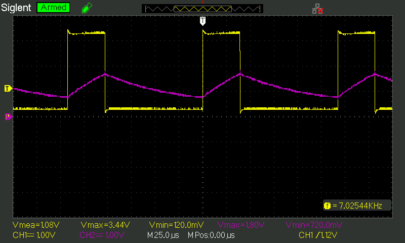
Note that the duty cycle is not 50%. In this particular circuit, it’s around 22%. Again, the math behind that is complicated. The duty cycle will be a function of the two threshold voltages, and I estimate between 20-30% depending on the Schmitt inverter that you use.
The circuit itself is very easy to build with a small footprint. (If you already use an inverter in your circuit design and have a spare gate, use a Schmitt chip instead and you get this for no extra cost in footprint.) The cost of a single resistor and capacitor is trivial. And you can easily modify the frequency of operation by changing R and/or C. The limitations on the frequency will mostly depend on the largest capacitor you can use. You could easily get away with an electrolytic capacitor (because the voltage doesn’t ever go negative), so a few hundred uF are possible.
A photo of the circuit itself is shown below. Note the nice small footprint.

Limitations of this type of clock source are going to be similar to what we see with a 555 timer. You’re somewhat limited by component values, although a trimmer potentiometer can be used to help account for any issues with component values and/or tolerance. Any device using resistors and capacitors will have varying properties if large temperature fluctuations are possible, so that’s a possible downside.
Crystal oscillator
A quartz crystal is simply a piece of quartz that resonates (vibrates back and forth) due to its internal crystalline structure. It’s piezoelectric, which means that these mechanical vibrations yield tiny little changes in voltage. If you’ve ever owned a quartz watch (or other timepiece), that simply refers to the crystal inside of the watch that’s keeping time. You can buy crystal oscillators online; these are specifically manufactured to have a particular resonant frequency and are packaged into a piece that can be soldered or wired into a circuit design. (Jameco has multiple frequencies of crystal oscillators, and the cost is less than or around $1 depending on what you want.) Quartz crystals have the advantage of being extremely precise at timekeeping. This means a quartz-based design is going to have the most stable output response of any of the clock signals presented in this post.
The voltage output from a quartz crystal isn’t going to naturally swing between 0V and 5V, so you can’t simply take a quartz crystal and plug it in as a clock source. However, it can be used as the timekeeping component of a circuit that does generate a clock source.
I’ve seen many schematics both online and in books for circuits that generate clock sources. Specifically, I have looked into TTL circuits, as that’s what I use in every (true with very minimal exceptions) digital logic circuit I build.
I joke that the term “it can be easily shown” is used by authors when they either can’t explain the derivation of something complicated, or just don’t feel like including an extremely complicated derivation in their work. Most every article I’ve read about TTL clock sources from crystal oscillators are of the “it can be easily shown” variety. Which means that I build them and nothing works. This made me feel inadequate as an electrical engineer. If all these random Internet strangers can do it, why can’t I? How hard can it be? If it’s so easy, why is nothing happening? I then found an application note online that validated my experience: “Although these types [of circuits] are popular, they are often associated with temperamental operation, spurious modes or outright failure to oscillate.” I’m glad the engineer who write the application note was able to outright say that crystal oscillators are complicated, and you really can’t expect a circuit to work without a robust understanding of the physics and engineering behind them.
As I don’t particularly care to obtain my own robust understanding of this operation, I really don’t feel like spending an enormous amount of time and energy to figuring out how to get these “it can be easily shown” circuits to work. I will show you a representative example (shown in the figure below) of “clock output” that I am capable of getting with the circuit in Figure 1c in that application note. It would not be capable of clocking a digital logic circuit, so it’s really not worth exploring any further for me.
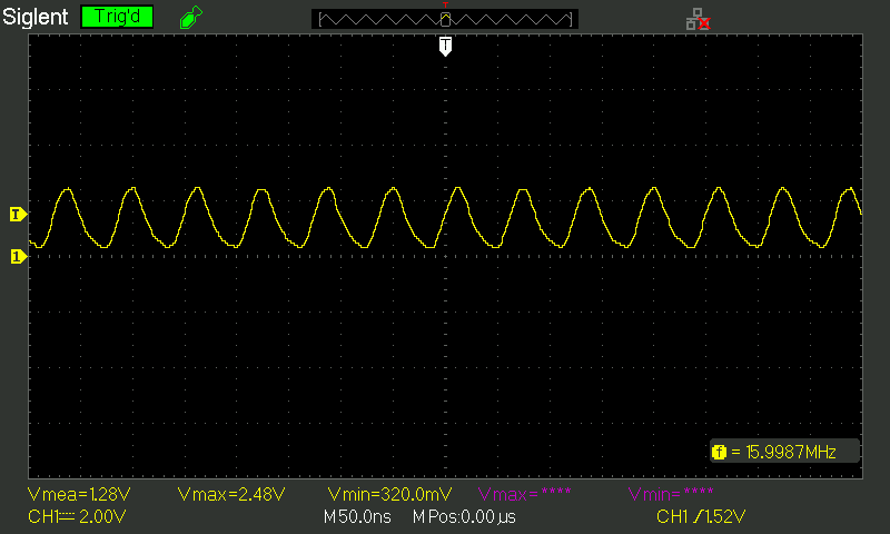
I used a 16 MHz crystal, so it makes sense that the oscilloscope is clocking a 16 MHz frequency in the output response. But it’s not a square wave, and the logic levels are not TTL. If I use a Schmitt inverter to try to clean that up, it breaks the black magic and stops working. 🤷🏻♀️
Fortunately, as it turns out, in the modern era, there is no need to use a crystal oscillator in a circuit like this. Keep reading to find out why!
Microcontroller
These days, microcontrollers are ubiquitous. You can purchase one for a few dollars, program it, and have it doing some pretty amazing things within minutes. (Depending on your programming ability “minutes” may be more like “hours” or “days.”) I thank the Arduino for spearheading this revolution. There’s no need (for the hobbyist, at any rate) to buy expensive IDEs, breakout boards, or developer kits anymore.
This means that you can take a microcontroller and use either its internal oscillator or an external crystal to generate a clock source, all using the internal circuitry of the microcontroller itself that is capable of performing the crystal oscillator black magic and using it to clock the CPU of the chip.
I used two different microcontrollers to demonstrate this. The first I selected was the ATtiny85, which I picked purposefully because it’s a DIP-8 chip, which means it’s the exact same size as a 555 timer (and smaller than the 7414 Schmitt inverter chip). That means in the same exact footprint of the 555 timer I can get some pretty great clock generation possibilities without the need for any other external passive components. I can use a crystal oscillator if I want a specific frequency, otherwise I can use the internal oscillator and still have a ton of options.
The ATtiny85 has a built-in 8 MHz oscillator. This can be output onto an I/O pin as-is, providing access to a nice TTL-compatible square wave. In addition, the 8-bit timer/counter can be utilized to divide this by any integer between 1 and 242,144. This yields frequencies between 30.5 Hz and 8 MHz. That’s pretty robust!
Alternatively, if you have your own crystal that you want to use, you can connect it to the microcontroller and use it as a clock source. Unfortunately, due to the pinout limitations of the chip, you won’t be able to generate a square wave at the oscillator frequency… the fastest you can get is the oscillator frequency divided by 2. (This is because things only happen as fast as the clock, so if I want to toggle an I/O pin, I can drive it HIGH the first time the oscillator ticks, and then LOW the next time the oscillator ticks, but now I’ve divided the clock by 2.) There is a CLKOUT pin that we can use (that outputs the clock signal directly to an I/O pin), but it shares one of the XTAL pins, so you can’t use it if you’ve got an external crystal connected. Bummer!
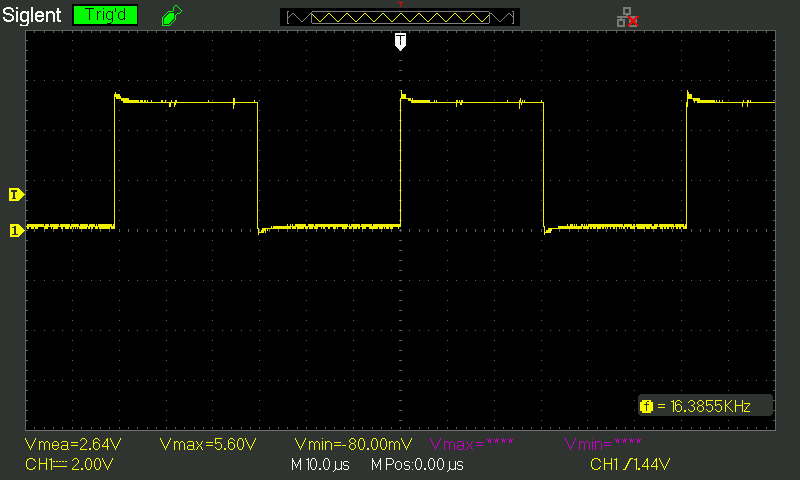
I used a 32,768 Hz crystal oscillator (the silver cylinder in the circuit) connected to an ATtiny85, shown in the figure below. Note the tiny footprint.

The range of allowable frequencies is still pretty robust when using the timer/counter, as it allows you to divide the clock by integer values up to 242,144. The output of the clock source (divided by 2) is shown below. Note the frequency is roughly 16,384 Hz.
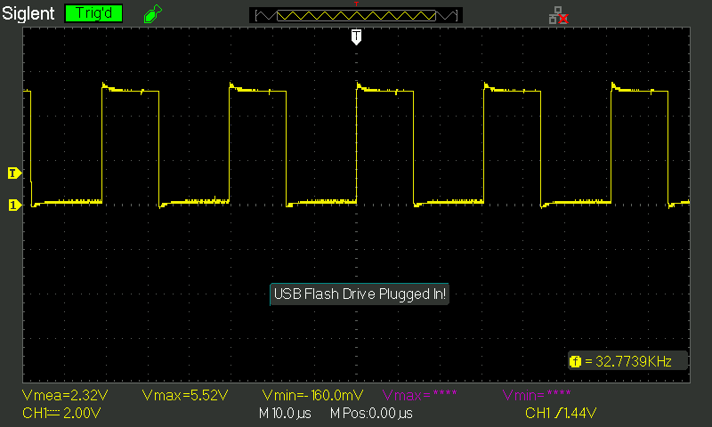
If you do want the possibility of using the CLKOUT pin to get an exact frequency from an external crystal oscillator, you can sacrifice the footprint size and make this happen. The ATtiny44 is a DIP-14 microcontroller that has a CLKOUT pin separate from the two XTAL pins. It’s still a pretty small footprint considering the other designs presented in this post. A photograph of the circuit is shown below. I used the 32,768 Hz crystal again.

The oscilloscope trace showing the output of 32,768 Hz is shown below. (Sorry about the USB drive message, I didn’t realize it was there when I printed the screen to an image until after I had taken everything apart and cleaned up my desk, and I don’t feel like rebuilding it.)
(Side note: you may be wondering why 32,768 Hz. It’s such a specific frequency! The reason is if you use a 15-bit counter to divide it, you get a frequency of exactly 1 Hz. So these crystal oscillators are commonly used in real-time clock circuitry.)
Conclusion
This was a fun way to learn about some new (to me) ways to generate clock signals. In my digital systems class, I see no reason to stop using the 555 timer, as it has both the versatility and ease-of-use that’s necessary in an intro class.
However, in my own circuit designs, I see no reason why I couldn’t pivot to using an ATtiny85. It’s got a nice small footprint and will likely eliminate the noise issues I get with a 555. A benefit to the 555 timer is that you can inhibit the clock with a single electrical signal. I could probably achieve something like this at the cost of a little extra software (no hardware would be needed) with the ATtiny85 as well, although I haven’t put that into practice at this point.
Alternatively, if I have a design with a 7404 and at least one extra unused inverter, I could easily swap it with a 7414 chip and obtain a clock signal with only one resistor and capacitor (as long as the timing works out) with pretty much no addition to my footprint. This might be a great option when those criteria are met.
